|
Leading the industry with high value-added products by our accumulated technological capabilities
Japan Science Engineering Co., Ltd.
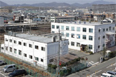
Muko City, Kyoto Prefecture
Mr. Mitsuzo Okamoto, Representative Director
|
|

|
|
| Location |
: |
1, Kuguso, Terado-cho, Muko City, Kyoto 617-0002 |
| Established |
: |
February 1967 |
| Business Description |
: |
Design, manufacture and marketing of precision equipment, physical and chemical instruments, measuring devices and optical devices |
URL |
: |
https://www.kakenjse.co.jp/ |
|
Nagaokakyo was a city built by the order of Emperor Kanmu around 1200 years ago. Nagaokakyu, the center of Nagaokakyo, was in what is now Muko City in Kyoto Prefecture. We visited Japan Science Engineering Co., Ltd. in Muko City. We asked about quality-focused manufacturing that has been maintained over the long history of the company which has excellent optomechatronic technology, fusing optical, electrical and precision machines and constantly leading the industry.
Increased their presence with maskless exposure device
Mr. Koji Okamoto,
Senior Managing Director
|
Japan Science Engineering Co., Ltd. (Hereinafter referred to as Japan Science Engineering) is a manufacturer that develops and manufactures exposure devices that form micro circuit patterns for electronic components. There are exposure devices for every purpose, but the specialty of Japan Science Engineering is exposure devices for LCD and FPD (Flat Panel Display) for mobile phones and for LED. Mr. Mitsuzo Okamoto, who is the representative director of Japan Science Engineering, talked about the company business as follows.
“Our company was manufacturing exposure devices for semiconductors at the time of the company's founding in 1967. After that, our operations expanded since the company shifted toward exposure devices for FPD and LED manufacturing due to the entry of major manufacturers in the industry.
In recent years, our company is increasing our presence in the field of maskless exposure technology that does not use photo mask as the original plate of the circuit pattern.” Mr. Koji Okamoto, who is the senior managing director of Japan Science Engineering, emphasized their technical advantages as follows.
“The processing accuracy of general maskless exposure devices for printed substrate is from around 20 to 30 µm. On the other hand, our company had a higher-level processing technology achieving processing accuracy from 7 to 9 µm from the beginning. Currently, our technology is further improved and achieves micro processing of 1 µm.”
Confidence in systems of development and quality assurance
Mr. Toru Endo,
Manager in charge of
the department of production
and technology
|
It is noteworthy that almost all exposure devices developed and manufactured by the company are made to order. Mr. Toru Endo, who is the manager in charge of the department of production and technology, talked as follows.
“Since required functions are different depending on the customers, it is usual for us to design them one by one after receiving orders for devices and then to manufacture them. Special orders from customers often become challenges leading us to develop new technology and even now we are working on film sensors. For our part, we just feel like manufacturing together with customers.”
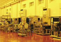
What makes one by one manufacturing of devices possible is the enhanced development system in the first place. Optical, electrical and precision machine technologies required for exposure devices are developed in-house and the number of development personnel accounts for one-third of all employees.
In addition, it is also noteworthy that the perfect quality assurance system increases the added value of products.
The manager in charge of the department of production and technology, Mr. Endo, says “The components used for each product are slightly different since they are not mass-produced products. Considering such circumstances, we are working hard on enhancement of quality assurance levels by increasing our inspection know-how step by step.”
Mr. Masaki Kishida,
Technology assistant chief of
the division of quality control of
the department of production
and technology
|
Mr. Masaki Kishida, the technology assistant chief of the division of quality control of the department of production and technology, and one more person are in charge of inspection work. Mr. Kishida, who has been doing this inspection work for 16 years, takes charge of components requiring higher dimensional accuracy and other staff is in charge of components for which the measurement method is established.
Mr. Kishida talked about difficulty in inspection work as follows.
“In terms of machining accuracy, we have confidence in our partner companies that we ask for component machining. However, if the requested accuracy is not satisfactory, it is necessary to clearly tell them that we cannot accept it. At that time, it matters how we tell them. If we just say that it is probably not good, the person who actually machined the component will never accept it. It is vital that we obtain accurate measurement results and logically explain the reasons based on them. It is the responsibility of those of us who perform the inspection work while standing between our development personnel and partner companies. It is essential for us to thoroughly perform the inspection work in order to secure the accuracy such as by measuring a single component using various methods.”
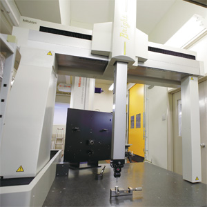
Newly introduced high accuracy CNC CMM
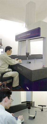
|
Mitutoyo’s high accuracy
CNC CMM STRATO-Apex 9106
|
When visiting the inspection room on the first floor of the headquarters, many measuring machines including Mitutoyo’s CNC CMM Bright-Apex, CNC vision measuring machine QUICK VISION-Apex (equipped with touch probe) and roundness measuring machine ROUNDTEST RA-2200 are installed. The most eye-catching was the horizontal CMM CARBstrato. We heard from the company that this machine was used for development and manufacturing of one of the world’s largest exposure devices for FDP.
In addition, the high accuracy CNC CMM STRATO-Apex 9106 that was newly introduced in January 2019 was there.
Mr. Kishida mentioned about the advantages with the high accuracy measurement using scanning probes in addition to the high measurement accuracy as the reason why they selected this machine.
“Measurement using the touch probe was one of the causes of measurement error since it can deform the workpiece due to measurement pressure.
In that respect, we are expecting to eliminate these measurement errors that occurred before since STRATO scanning measurement offers fine sensing to obtain measurement values. As mentioned above, it is a great advantage that we can show measurement results with confidence.”
Japan Science Engineering is taking a strong approach to quality assurance along with the company's motto: “On the volume, do not try to be the maximum. On the quality, strive to be the best.” Mr. Okamoto, Representative Director, said “Continuing to focus on this motto is our permanent theme for achieving sustainable growth.”
“Manufacturing of development-oriented products is the core of our business. We will continue to strive in order to manufacture quality products that can fully satisfy customers.”
Representative Director Okamoto mentioned that work toward new product areas will be the theme of their business.
“This requires improving each employee's ability. While improving ourselves, we gather together to be a strong team.” He said this with enthusiasm.
Japan Science Engineering continues to improve their technology and quality that are already at a higher level by sustaining their work and converting deep trust from customers into a motivating force. They will continue to make great strides.
|
|
|
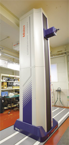
Mitutoyo’s horizontal-type CMM
CARBstrato |
Mitutoyo’s CNC CMM
Bright-Apex |
|
|